
Laser-PSFL Masking Technology


Laser-PSFL Technology
3t Technologies Limited is an advanced product development and technology innovation company located in Essex in England specialising in thin (and thick) film electronic device process and manufacturing development applicable to a wide variety of device technologies.
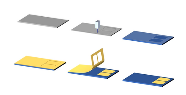
3t's core technology is Laser precision patterned Peelable Solid Film Lithography masks [Laser-PSFL], a process that simplifies additive deposition coating patterning in device manufacture. It is aimed at providing a more versatile alternative to current selective area masking processes such as photolithography patterned photo resin coating masks and fine metal masks for R&D and appropriate manufacturing applications. A typical Laser-PSFL mask held by tweezers and an illustration of its use in providing metal contacts for thin film material Transmission Line Method measurement is shown below. Other mask designs and masking materials are possible.


Laser-PSFL has several distinguishing features including:
-
Ultra-thin sheet film mask in soft intimate contact with the substrate
-
Cleaner and more user-friendly process than photolithography
-
All dry process
-
Used film mask is mechanically peel removed cleanly in sheet form

Laser-PSFL benefits include:
-
Device fabrication cleaning stages reduced
-
Easier used mask removal with retained residual coating material for efficient waste disposal (shown in lower left rectangle area in picture above, where the required pattern mask was produced)
-
Smaller hardware footprint (cleanroom space)
-
Lower cost consumables
-
Lower processing time for mask production with reduced labour cost per mask
-
Material heating stages eliminated
-
No toxic or hazardous liquid chemicals handling, storage, waste collection and disposal, or need for purchase of personal protective equipment to work with it
-
Overall capital equipment spending reduced
-
Processing steps reduced improving process efficiency and yield
-
Laser-PSFL mask patterning undertaken off-sample and transferred onto it with/without alignment depending upon the application requirement, so sample surface remains uncontaminated by the patterning process.
"Contact us today to discuss your application"