
PSFL Thin Film Patterning
"Transparent electrical contacts"
PSFL: Thin film coating patterning
PSFL technology is primarily aimed at low temperature (< 140 C : includes the temperature set on the substrate + the temperature induced by the depositing coating/process) whole or selected area thin film coating vapour deposition primarily using atmospheric and vacuum-based physical vapour deposition (PVD) processes. It provides direct additive coating patterning at the deposition process stage when the PSFL sheet film mask is mechanically peeled off after use (coated by the depositing thin film material).
A brief overview of the compatibility of PSFL technology with some examples of deposition processes and associated coating materials and substrates is provided below.
o
PSFL: Substrate materials compatibility
The PSFL film masks have been used on a variety of substrate types including:
-
Crystalline and ultra-thin polycrystalline silicon wafers – uncoated and coated (i.e., oxide and nitride)
-
Borosilicate and quartz glass plates and wafers
-
Plastic sheet film – uncoated and coated (i.e., transparent conducting ITO thin film coated)
-
Paper sheet – treated (i.e., polymer coated)
PSFL: Thin film process compatibility
The PSFL sheet film masks have been used with a variety of PVD thin film deposition processes including:
-
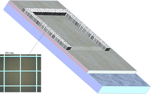
RF and DC magnetron sputtering (see picture on the right)
-
Remote plasma sputtering
-
Ion beam sputtering
-
Thermal and e-beam evaporation
-
Ion-assisted deposition (IAD)
o
PSFL sheet film masks are also compatible with some chemical vapour deposition (CVD) processes, such as PECVD and ALD, that provide suitable high-performance coatings at a low enough coating temperature (< 140 C : includes the temperature set on the substrate + the temperature induced by the depositing coating/process). Once the used PSFL film mask is removed ["peel-to-reveal" process], the remaining patterned coating is ready for use for the subsequent step in the device manufacture.

PSFL: Thin film deposited coatings compatibility
The PSFL film masks have been used to pattern a variety of thin film coatings, deposited at < 100 C : includes the temperature set on the substrate + the temperature induced by the depositing coating/process, including:
-
IGZO – TFT metal oxide semiconductor
-
CuO2 – PV metal oxide semiconductor
-
HfO2 – TFT metal oxide high-K gate insulator
-
ITO – Metal oxide transparent conductor
-
Metals including gold, pure and silicon-doped aluminium, chrome – Device electrical contacts and interconnections
Coating from a few nm to approximately 1.5 micron thickness (e-beam metallisation as shown in the picture on the right) have been patterned.
o

PSFL: Sheet film masks
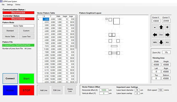
The 3t L3PM R&D system user interface window has a “pattern graphical layout” window that shows the pattern layout as constructed by the user prior to running the laser patterning process. The vector coordinate data used in the construction of the user pattern is shown in the “vector pattern table” which is located next to the pattern draw window in the picture below.
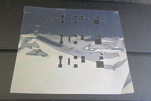
The picture on the right shows an ultra-thin PSFL sheet film mask in which the pattern shown in the L3PM system operating user interface graphics window has been step and repeated twice.
Some results from the early PSFL sheet film patterning process investigation of the laser – material interaction is shown in the picture below left. For this experimentation the laser spot size at the focal plane was 10 microns and no localised gas cooling or laser debris extraction was used.

The picture on the right shows the excellent edge quality and straightness of a line cut through a PSFL thermoplastic sheet film.
The melt ridge and heat affect zone are manipulable using the amount of laser energy absorbed and the degree of localised cooling applied during film aperture cutting.

The picture on the right shows a section of a PSFL sheet film mask supported on a plastic carrier film after undertaking laser aperture pattern cut-outs of various test devices (thin film fuses, microfluidic channels, etc.), but prior to patterned mask attachment onto a sample.
The picture shows a set of processing conditions that produce partial depth trenches cut into a plastic sheet film with no laser induced debris observed. The full-length line cut shown has a width estimated to be 12 ± 0.6 microns. The laser was operated in continuous wave (CW) mode and the excess energy absorbed has contributed to the formation of a melt ridge in the absence of cooling. The melt ridge has a smooth surface and provides improved tear resistance around the perimeter of a laser cut pattern aperture.

The picture on the left shows a section of a PSFL sheet film mask on a carrier film after laser dicing an array of square segments when testing the orthogonality of the system hardware.

The focused spot size can be readily changed by swapping out the focusing optics assembly on the laser module. Spot sizes of 10 and 6.3 micron have been evaluated but a size down to 2.5 microns is possible (although allowance for a depth of focus < 20 microns must be made).
PSFL technology advantages over standard photolithography
The PSFL advantages over the industry standard photolithography – UV patterned exposure liquid photo resin coating masking layer process, are listed below.
-
Attached patterned mask turnaround time [Reduced processing steps and separate patterning and alignment-attachment systems provides faster sample turnaround reducing equipment access bottleneck]
-
Cleaner processing [All-dry processing reducing need for rinse-dry cleaning steps]
-
Consumables cost saving [Dry consumable sheet film mask blanks provide savings because no liquid chemicals storage, handling, safety, processing equipment, personal protection equipment, waste collection and disposal, or cleaning steps associated with their use]
-
Consumables PPE [Personal protective equipment (PPE) – disposable clothing – is not required because no toxic or hazardous liquids are used with the PSFL technology]
-
Ease of mask handling [Simpler and cleaner consumable mask blanks making processing quicker, cleaner, and easier]
-
Easier residual precious metal collection [Gold vacuum deposited coatings can be used on samples where normally a high proportion of the mask surface area would be coated with the coating which would normally be lost. Because the residual coating on mask is efficiently collected as the used mask is cleanly peeled-off the sample after use it is much easier to collect the residual gold for subsequent processing to reclaim it]
-
Mask repositioning possible [Enables simpler rework if alignment is initially incorrect]
-
No on-sample patterning [Samples remain contamination-free and damage-free which removes the need to reclean, rework, or potentially scrap a sample]
-
No sample liquid exposure [Some substrates and samples with pre-coated layers on them can be sensitive to liquid exposure resulting in impaired performance or operation stability and lifetime of a manufactured device]
-
Reduced laboratory space requirement [No need for separate chemicals processing or drying equipment]
-
Reduced storage space [No liquid chemistry processing reduces the need for liquids storage]
-
Separate patterning and align-attach systems [Better access to the technology by separating out the patterning and alignment-attachment processes to allow parallel processing]
-
User safety [No toxic or alkaline liquids used in patterned mask preparation or used mask removal]
"3t is interested in working with companies that employ low temperature thin film deposition and associated coating patterning in device, component, and circuit manufacture, and who are early developers and adopters of innovative processing to advance our PSFL film masking technology and manufacturing capability for diversifying its industrial applicability."